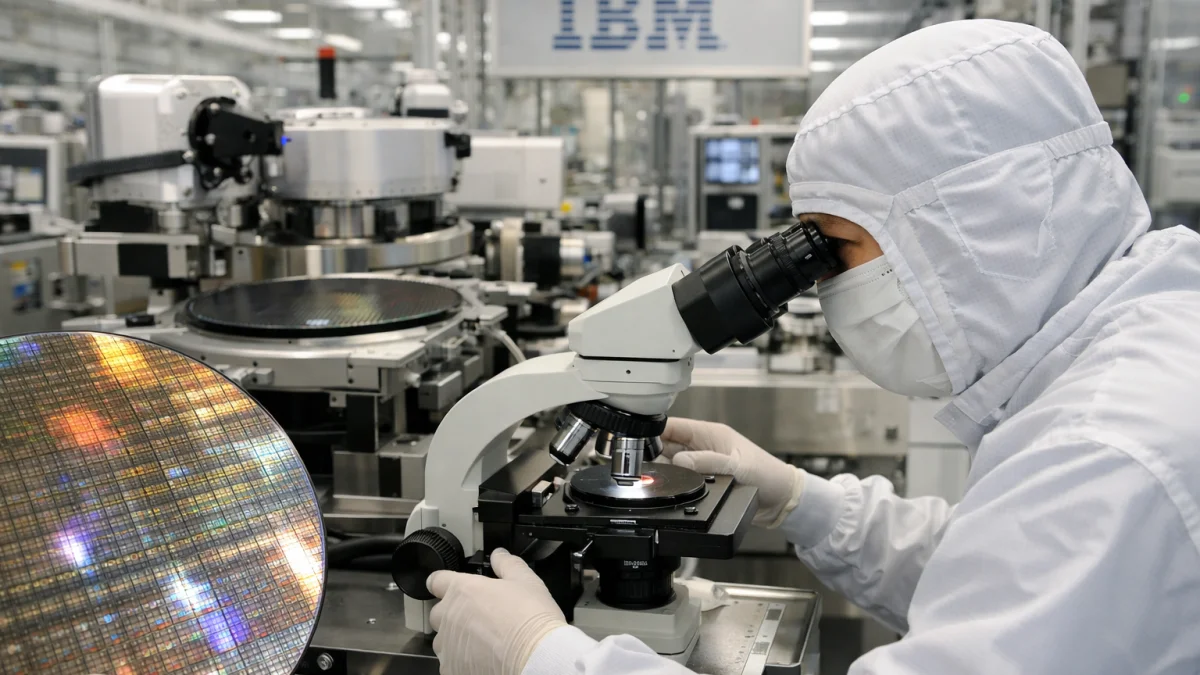
YORKTOWN HEIGHTS, N.Y. — IBM announced on Thursday that it has developed the world’s first sub-1 nanometer chip technology, featuring a transistor architecture at the 0.7 nanometer, or 7 angstrom, node.
The prototype technology uses a new “nanostack” 3D architecture that vertically stacks transistors in two layers, enabling nearly 100 billion transistors on a chip the size of a fingernail — roughly twice the density of IBM’s 2 nanometer technology unveiled in 2021.
IBM said the breakthrough is projected to deliver up to 50 percent more performance or 70 percent greater energy efficiency compared with its 2 nanometer node chips. The company described the advance as a step toward extending semiconductor scaling amid growing demands for artificial intelligence computing.
“IBM’s latest chip breakthrough marks a landmark moment in computing, pushing technology beyond the nanometer era to the scale of atoms,” Jay Gambetta, director of IBM Research, said in a statement.
The nanostack design builds on IBM’s earlier nanosheet technology and incorporates innovations in wafer bonding, SRAM scaling and channel materials. IBM Research presented the work as a research prototype, with commercial production potentially years away.
The announcement comes as the semiconductor industry faces physical limits in traditional scaling. IBM’s previous milestone, the 2 nanometer test chip, was revealed in 2021 and demonstrated the ability to fit about 50 billion transistors in a similar area.
Industry analysts noted that while the 0.7 nanometer label follows marketing conventions rather than a precise physical gate length, the vertical stacking approach addresses density challenges. IBM indicated the technology could reach production in about five years.
The development positions IBM’s research efforts in competition with major foundries such as TSMC and Intel in advancing process nodes for AI and high-performance computing. IBM does not manufacture chips at scale for external customers but licenses its technology.
As of Thursday, IBM had not released detailed timelines for manufacturing integration or specific customer applications. The company continues to collaborate with partners on related process technologies.